Design of General Antenna Matching Circuits
In antenna matching, the ideal scenario is to have consistent impedances at the source output, transmission line, and load input (generally around 50Ω).
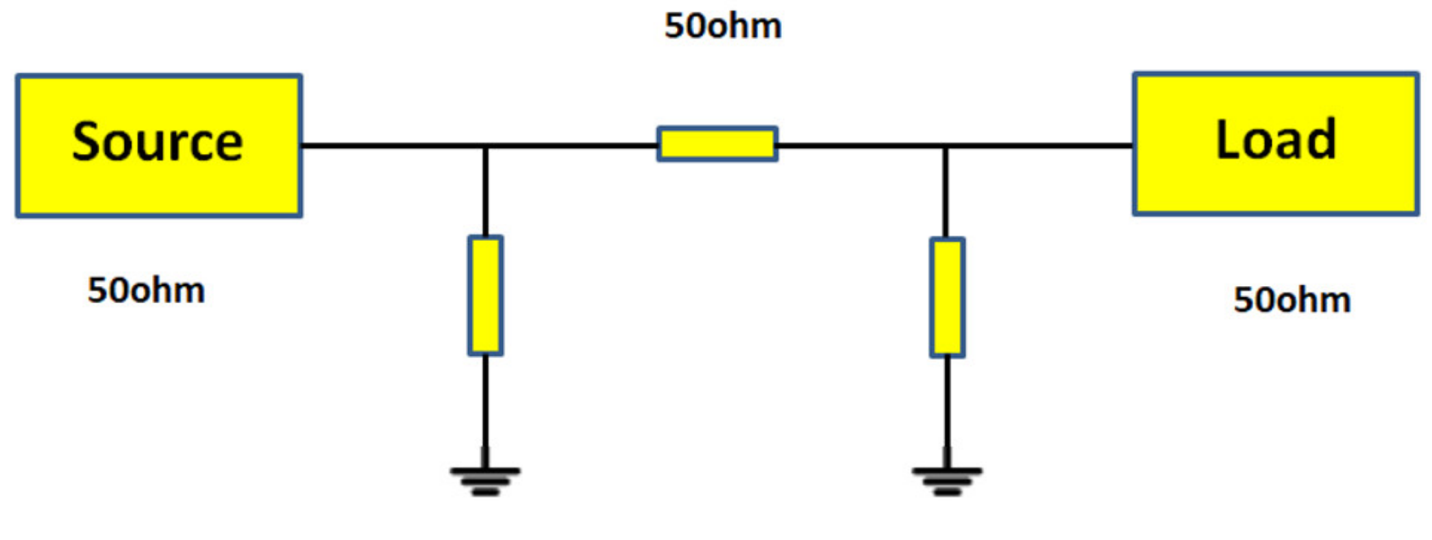
However, in practical situations, factors such as connectors, soldering, and errors in antenna impedance can lead to impedance mismatch beyond the source. Therefore, antenna circuits typically require the inclusion of matching circuits, often in the form of a π-type matching circuit, which will be explained in the following sections.
Measuring the Original Impedance
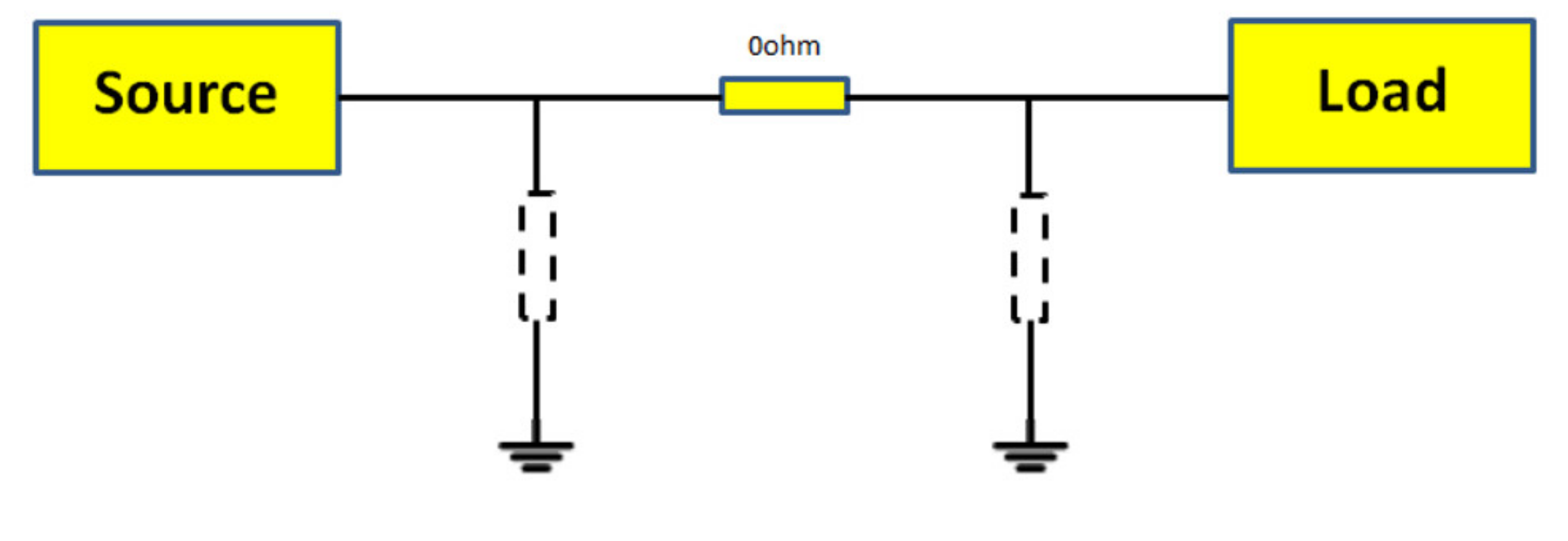
First, we need to understand the situation without any matching circuit. In this case, a π-type matching circuit involves soldering a 0Ω resistor (avoid direct soldering with solder, as it may result in different parasitic parameters) in series with the components at the source end and leaving the components to ground unconnected.
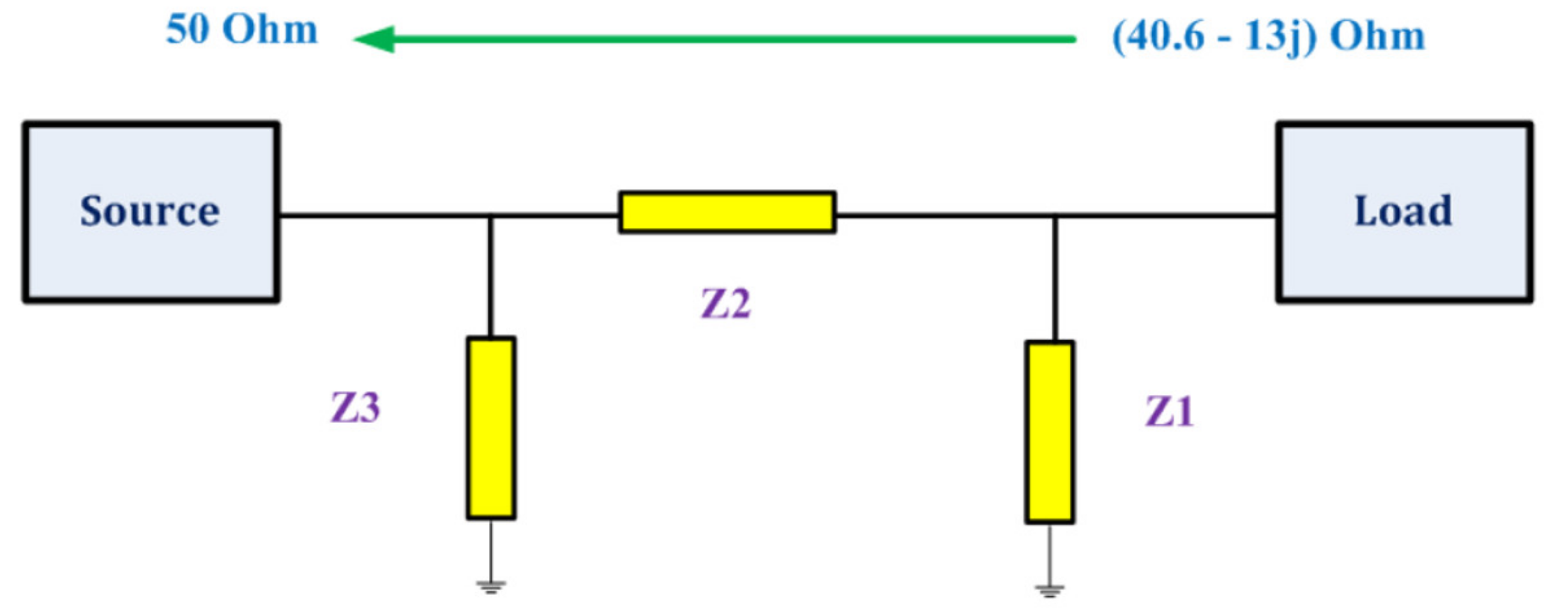
Measurements can be taken using a network analyzer, and you can refer to the article on Using Network Analyzers for specific methods. At this point, you can measure the initial load impedance. If the measured impedance is very close to 50Ω, you may not need a matching circuit, which not only reduces costs but also minimizes device-induced losses. However, if the measured impedance is (40.6-13j)Ω, the next step is to adjust the matching to bring the load impedance to 50Ω on the Smith chart.
Adjusting the Matching
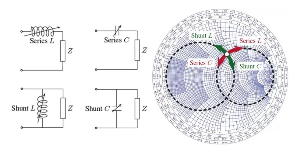
To adjust the matching on the Smith chart, you can use software like SimNEC. The principles of the Smith chart can be found in the article on Smith Chart Fundamentals. By adding components from the load end towards the source end, you can adjust the load impedance to 50Ω.
Principles of Matching:
- The inductance and capacitance values should not be too small (to reduce the impact of errors) and should preferably be common values (to increase interchangeability).
- The grounded capacitance value should not be too large (as larger values result in lower capacitive impedance, causing a significant signal to flow to ground).
- Design it as a low-pass filter if possible (which can also suppress high-frequency harmonics).
- Ensure that two inductors are not placed too close together, as this could affect the matching effectiveness through mutual inductance.
- Aim for the impedance trajectory to converge as much as possible across the entire frequency band.
- When designing the PCB layout, place the matching circuit as close to the antenna as possible to minimize transmission line delay, making the actual values closer to the theoretical settings.
References and Acknowledgments
Original: https://wiki-power.com/
This post is protected by CC BY-NC-SA 4.0 agreement, should be reproduced with attribution.This post is translated using ChatGPT, please feedback if any omissions.