How to Design a Minimal System for a Microcontroller
This article will explain the design process based on the STM32 microcontroller (F1 series).
Background
When learning embedded systems, we usually start with microcontrollers. To learn microcontrollers, it is not enough to only focus on software; hardware knowledge is also essential. The combination of software and hardware design is what makes a truly outstanding design.
When it comes to hardware design for microcontrollers, we first condense it into a minimal system, which is a simplified design that can achieve the most basic functions. Taking the STM32 (F1 series) microcontroller as an example, the minimal system consists of the following components: power supply, reset, clock, startup mode, and download/debugging.
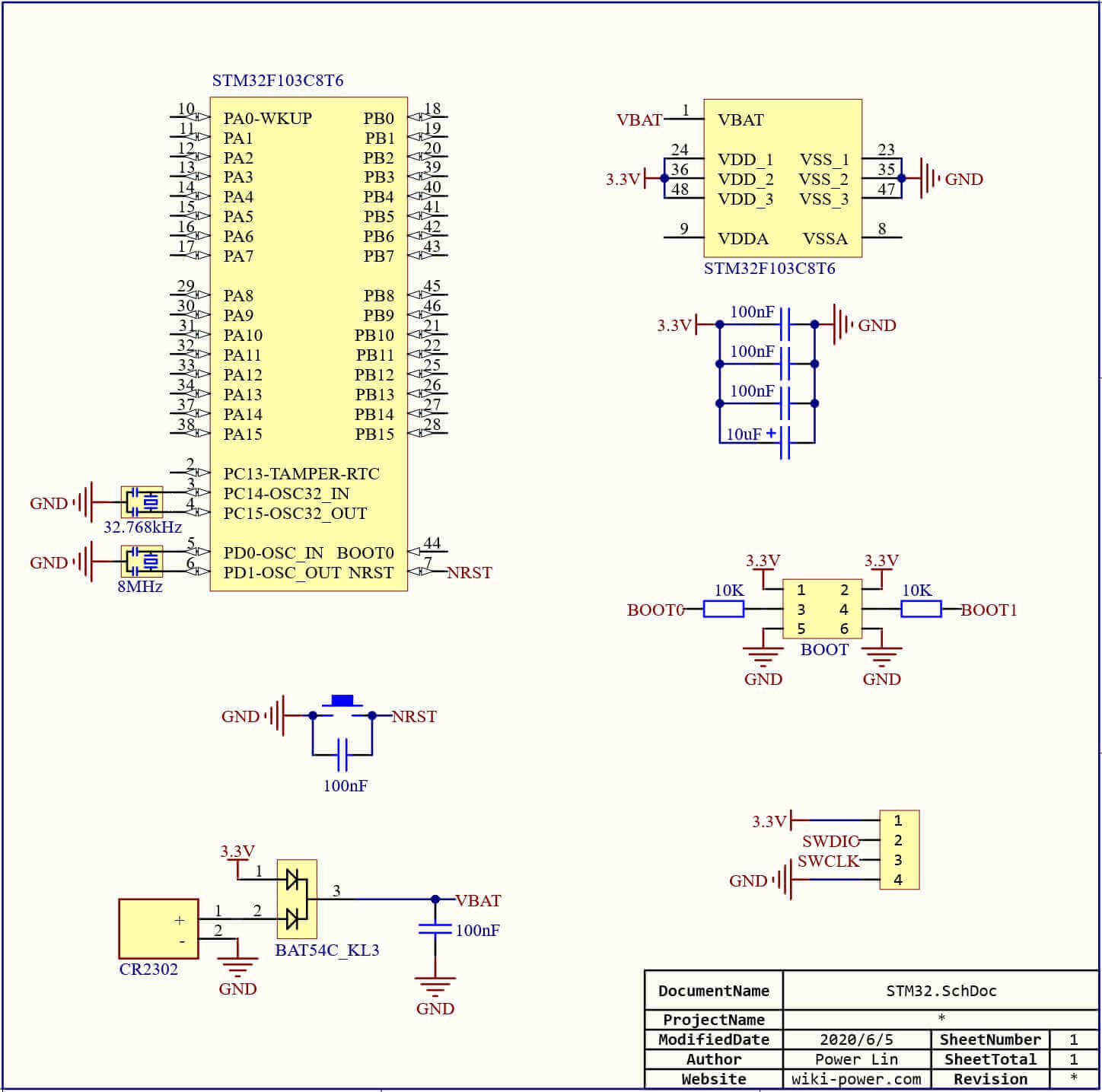
Power Supply
The STM32 microcontroller has the following types of power supply:
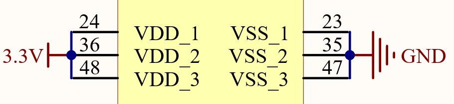
Main Power Supply (VDD / VSS)
The main power supply refers to the pins labeled as VDD1, VDD2, etc.
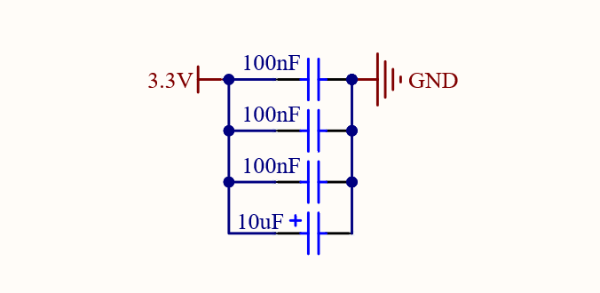
Each pin must be connected to a 100nF filtering capacitor, placed as close to the pin as possible. In addition, a shared 10uF tantalum capacitor is required.
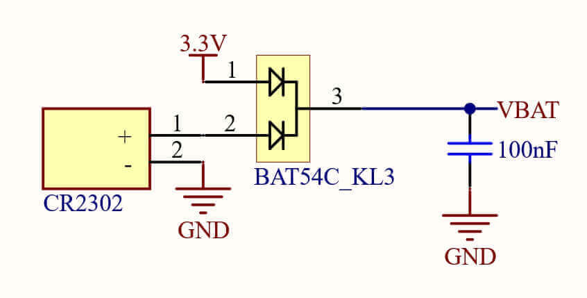
Backup Power Supply (VBAT)
The VBAT pin can be used for battery power. If not used, it can be connected to VDD. The VBAT pin also requires a 100nF capacitor for filtering.
Refer to the following power supply selection circuit:
ADC Power Supply (VDDA / VSSA)
To improve conversion accuracy, the ADC device can be powered from here. Generally, VDDA is connected to VDD through an inductor.
If ADC is not used, VDD, VDDA, and VREF+ (if available) can be connected together, and a 1uF tantalum capacitor + 10nF ceramic capacitor can be connected to ground for filtering.
Reset
Since the STM32 microcontroller has internal pull-up resistors, only an external 100nF capacitor and a button are required:
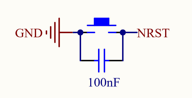
When powered on, the CPU is in a reset state. At this time, the capacitor charges, keeping the NRST pin at a low level. When the capacitor is fully charged, the NRST pin transitions to a high level, and the CPU exits the reset mode and enters normal operation. When the button is pressed, the capacitor is discharged, clearing the charge, and when the button is released, the capacitor is recharged, triggering a reset.
According to the official design guidelines, a 100nF capacitor is sufficient to ensure that the low level of NRST lasts for the minimum pulse width required for CPU reset, thus triggering a reset correctly.
If manual reset functionality is not needed, the button can be omitted.
Clock
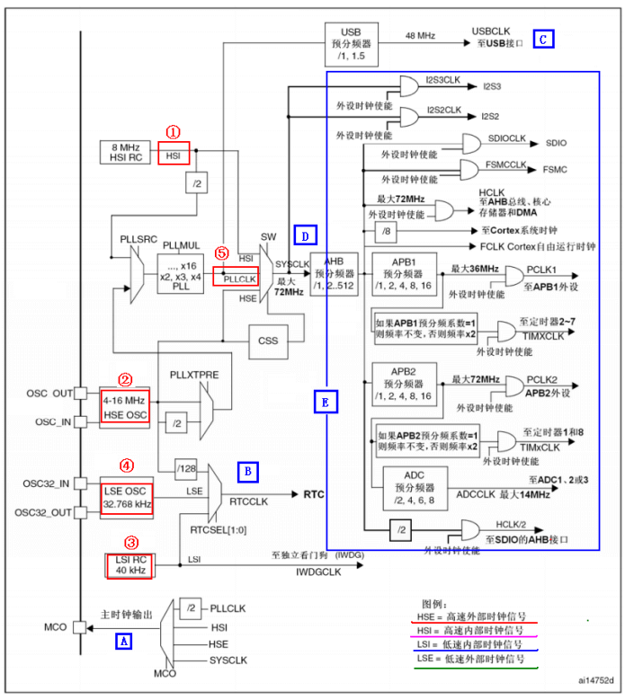
As shown in the above diagram, the STM32 microcontroller has the following types of clocks:
- HSI: High-Speed Internal clock, an internal RC oscillator with a frequency of 8MHz.
- HSE: High-Speed External clock, can be connected to a quartz/ceramic resonator or an external clock source, with a frequency range of 4MHz to 16MHz.
- LSI: Low-Speed Internal clock, an RC oscillator with a frequency of 40kHz. It can only be used as the clock source for the independent watchdog and can also be used as the clock source for the RTC.
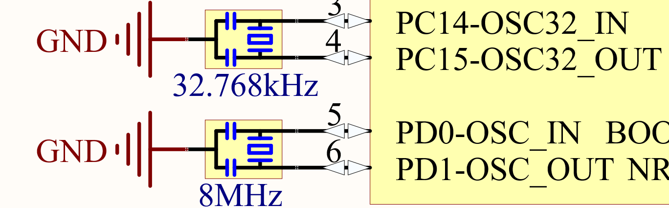
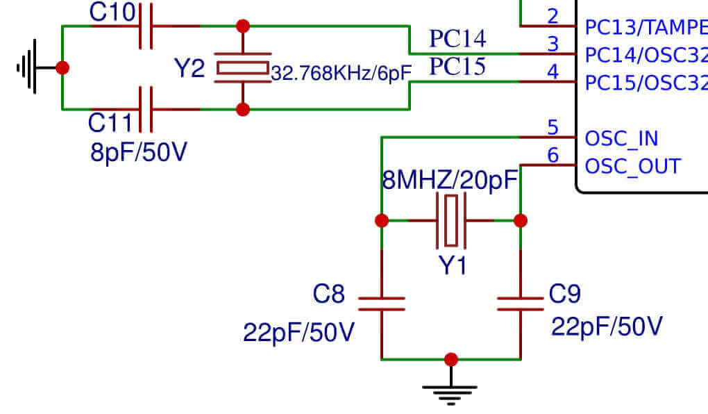
- LSE: Low-Speed External clock, connected to a quartz crystal with a frequency of 32.768kHz. LSE is used as the clock source for the RTC.
- PLL: Phase-Locked Loop multiplication output, with clock input sources selectable as HSI/2, HSE, or HSE/2. The multiplication factor can be 2 to 16, but the output frequency must not exceed 72MHz.
Considering stability, we generally use an external crystal oscillator as the clock source during design. An 8MHz crystal oscillator is commonly selected as HSE for easy multiplication (usually up to 72MHz); a 32.768kHz crystal oscillator is selected as LSE for RTC use and easy division (32768 is 2 to the power of 15, providing accurate time).
As for the choice of crystal oscillator, active ones have higher accuracy, while passive ones have lower cost, and passive ones are generally sufficient.
If a passive crystal oscillator is chosen, capacitors should be added at both ends to filter out high-frequency noise in the crystal oscillator waveform. The capacitance value can be selected from 10 to 40pF.
Add a 1M resistor between the crystal oscillator input and output pins to generate negative feedback and ensure that the amplifier operates in the high-gain linear region. It also acts as a current limiter to prevent the crystal oscillator from being overloaded and damaged by the inverter.
Boot Mode Configuration
Generally, pull down the BOOT0 pin (connect a 10K resistor in series and then ground it), and BOOT1 can be left floating.
If mode switching is required, you can refer to the following design:
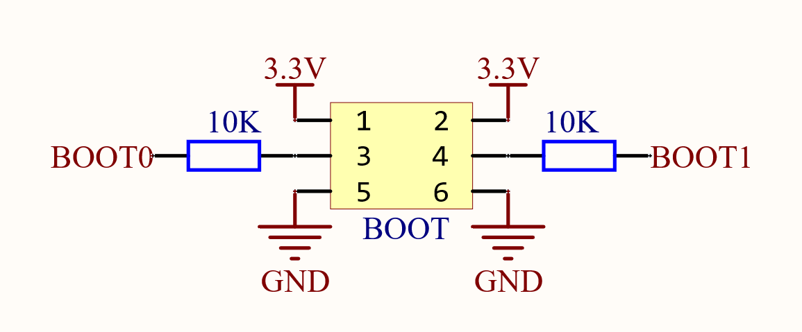
For more details about boot modes, please refer to Boot Modes of STM32
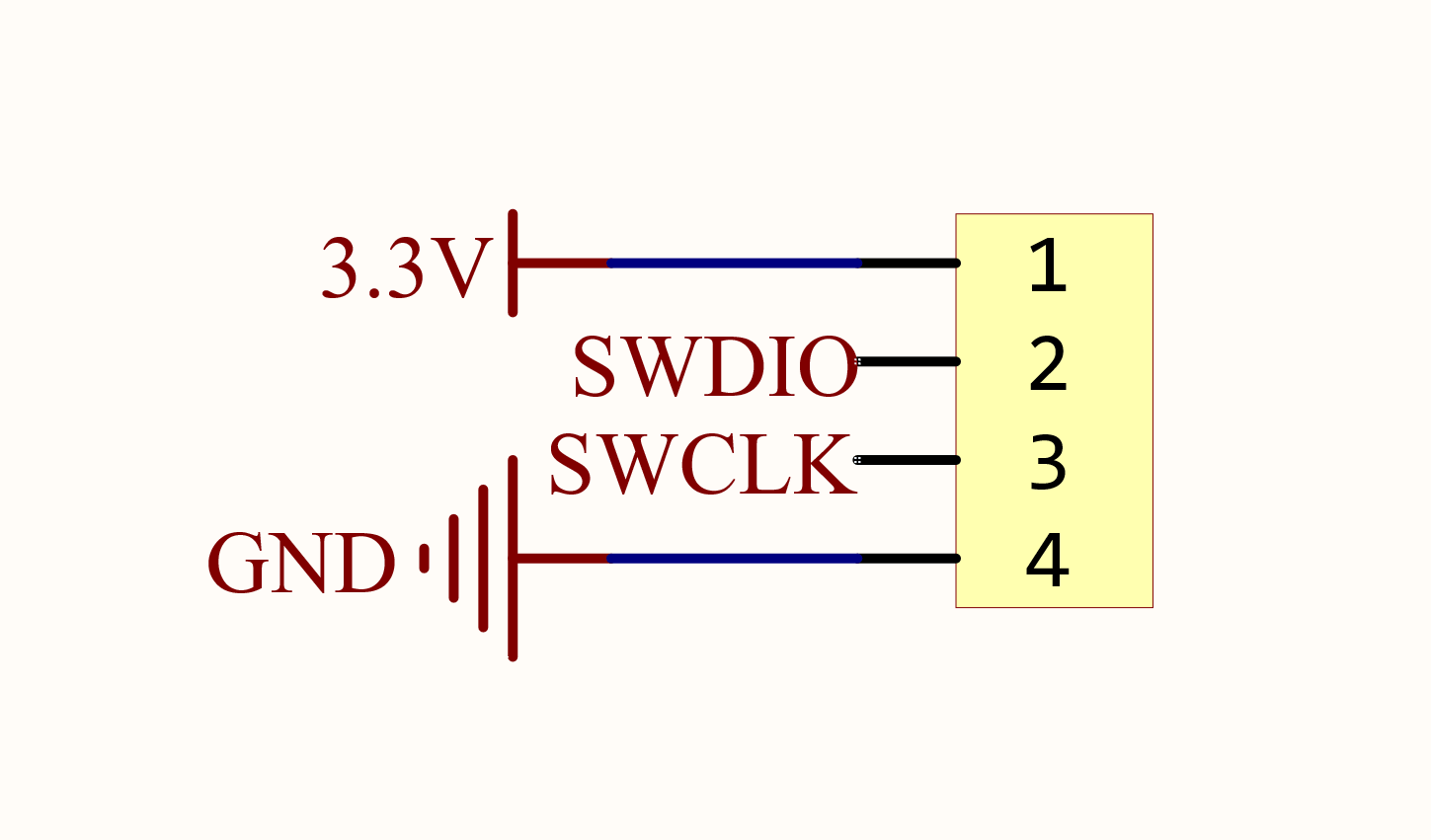
Download and Debug Interface
Generally, we use the SWD interface (fewer connections, more convenient), directly connect SWDIO, SWCLK, VCC, and GND. There is no need to add external pull-up/pull-down resistors because they are already integrated in the STM32.
Summary
The above is the circuit design of the STM32 (F1 series) minimum system. For more detailed content, you can refer to the official documentation and related articles below.
References and Acknowledgements
- Hardware Design Methods for STM32F1 Series Microcontrollers
- STM32 Hardware Design
- STM32 Clock System
- "AN2586 Application Note - STM32F10xxx Hardware Development Getting Started"
- "AN2867 Application Note - ST Microcontroller Oscillator Circuit Design Guide"
Original: https://wiki-power.com/
This post is protected by CC BY-NC-SA 4.0 agreement, should be reproduced with attribution.This post is translated using ChatGPT, please feedback if any omissions.