Motor Drive Solution - IR2104S
This motor drive solution is based on the half-bridge driver chip IR2104S and the AP30H80K N-MOS tube. The external voltage regulator for powering the IR2104S is implemented using the XL2009E1 solution.
Project Repository: Collection_of_Motor_Driver_Design/DC_Motor/IR2104S
Project Online Preview:
Basic Parameters
- Input
- VM: Input 12-36V, power supply for the motor (determined by the parameters of XL2009E1, IR2104S, and AP30H80K).
- VCC_3V3: Input 3.3-5V, external input voltage for the H-bridge system (determined by the parameters of the logic chip SN74LVC1G08DCKR).
- IN1/IN2: External logic inputs, recommended to follow the voltage of VCC_3V3, truth table shown below.
- PWM: PWM input, voltage level consistent with IN1/IN2.
- SD: Default internal pull-down, low level effective (turns off the IR2104S half-bridge chip), external input high level (VCC_3V3 voltage) turns on the IR2104S.
- Output
- M+/M-: Connect to the external motor.
- VCC_12V: On-board XL2009E1 circuit voltage regulator output, used as a backup power supply output.
When using the motor drive module, the H-bridge system needs to be grounded with the external controller.
The truth table for the logic control in this solution is as follows:
| SD | IN1 | IN2 | PWM | Motor State |
|---|---|---|---|---|
| 0 | x | x | x | Coasting |
| 1 | 1 | 0 | 1 | Forward |
| 1 | 0 | 1 | 1 | Reverse |
| 1 | 1 | 1 | x | Brake |
| 1 | 0 | 0 | x | Brake |
| 1 | x | x | 0 | Brake |
Basic Principles
Logic Circuit
To drive a motor, two pairs of half-bridge circuits are needed to form an H-bridge full-bridge circuit. In order to control the motor state according to the truth table, two AND gate circuits are used here to perform the AND operation between the external PWM signal and IN1/IN2, and the result (PWMA/PWMB) is passed to the IN pin of IR2104. The power supply input of the logic chip is decoupled with a 100nF capacitor.
Voltage Stabilization Circuit
The voltage stabilization circuit is built based on the XL2009E1 Buck chip, which functions to stabilize the external power supply input to 12V for powering the IR2104S chip (whose power supply range is 10-20V).
For the design of the voltage stabilization module, please refer to the article Power Solution (Buck) - XL2009E1, which will not be elaborated here.
Half-Bridge Drive Circuit
For the basic knowledge of motor drive, please refer to the article Design of Brushed DC Motor Drive, which will not be elaborated here.
IR2104S is a half-bridge driver chip from Infineon. Its main parameters are as follows:
- Floating bootstrap withstand voltage of up to +600V
- Gate drive supply voltage of 10-20V
- Compatible with 3.3V/5V/15V logic input levels
- Other features:
- Undervoltage lockout
- Integrated dead time control
- Cross-conduction prevention logic
- In-phase relationship between high-side and logic inputs
- Both high-side and low-side switches are turned off during shutdown
- Propagation delay matching between high-side and low-side switches
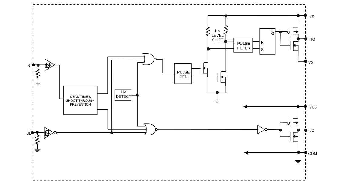
Internal block diagram:
Typical application schematic:
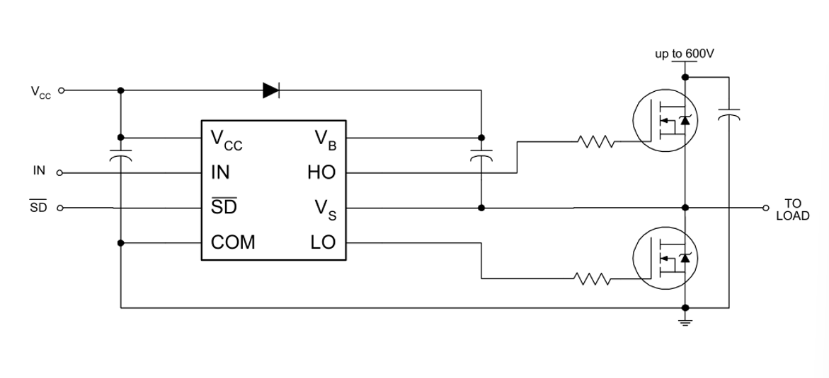
In this design, the IR2104S is powered by 12V and is connected in parallel with a 100nF input decoupling capacitor. IN is the logic input pin, where input above 3V is considered high level and below 0.8V is considered low level. The PWMA/PWMB high and low level signals, generated by the logic chip, control the switching on and off of the high-side and low-side switches. SD is the external shutdown input (active low). The timing diagram for the IN and SD mixed inputs, corresponding to the HO/LO status of the gate pins of the high-side and low-side switches, is as follows:
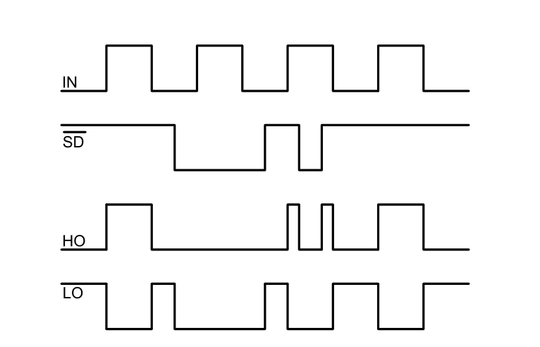
As can be seen, if the IN input is high, the high-side gate is driven high and the low-side gate is driven low, and vice versa. If SD detects a low level, regardless of the IN input level, both high-side and low-side switches will be pulled low to turn off.
To prevent shoot-through of the high-side and low-side switches on the same half-bridge, the IR2104S integrates dead time control. The timing diagram for dead time control is as follows:
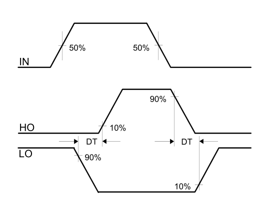
Where DT has a typical value of 520ns.
Timing diagram for high-side and low-side switch turn-on/turn-off:
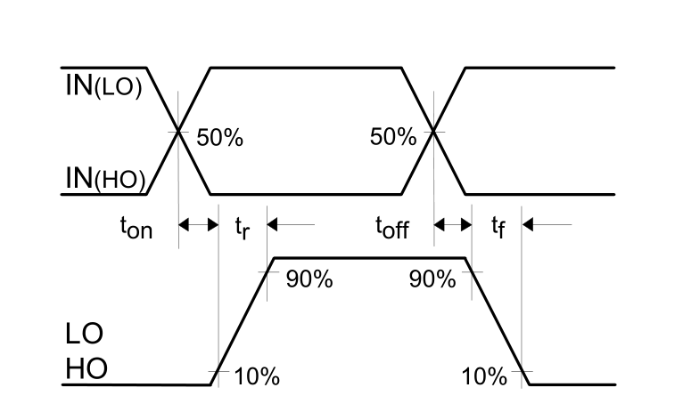
Where the typical values for \(t_{on}\) and \(t_{off}\) are 680ns and 150ns, respectively.
Because N-MOSFETs are used in this design (the conduction condition is \(V_g-V_s>V_{gs(th)}\)), a high-side floating bootstrap circuit is required to properly turn on the high-side switch. This design uses a 1uF/50V MLCC capacitor connected between the VM and VB pins, which raises the voltage at the HO pin above the N-MOSFET's \(V_{GS(th)}\), i.e., the IR2104S supply voltage minus the forward voltage drop of the diode, allowing the high-side switch to turn on properly.
The selection of the MOSFET needs to consider parameters such as \(V_{DSS}\), \(V_{gs(th)}\), \(I_D\), and \(R_{DS(on)}\). \(V_{DSS}\) is determined based on the motor's voltage plus a sufficient margin; \(I_D\) is determined based on the application's requirements with an additional margin; and a smaller \(R_{DS(on)}\) is better. Taking into account the parameters and price, this design uses the AP30H80K.
For the freewheeling mode design, since the IR2104S does not integrate synchronous freewheeling, we use the SS34 Schottky diode for asynchronous freewheeling.
References and Acknowledgements
- Detailed Explanation of H-Bridge Motor Drive Circuit with STM32 and IR2104S
- Doubts about Bootstrap Capacitor for MOSFET H-Bridge Driver Chip
- AN-6076 Design and Application Guide for High-Voltage Gate Driver IC Bootstrap Circuit
- Why PWM for Motor Control Cannot Be Too Fast_【Motor Control】Why Can't the Complementary PWM Control of the Upper and Lower MOSFETs Have a 100% Duty Cycle?
Original: https://wiki-power.com/ This post is protected by CC BY-NC-SA 4.0 agreement, should be reproduced with attribution.
This post is translated using ChatGPT, please feedback if any omissions.