Power Solution (PMIC) - EA3059
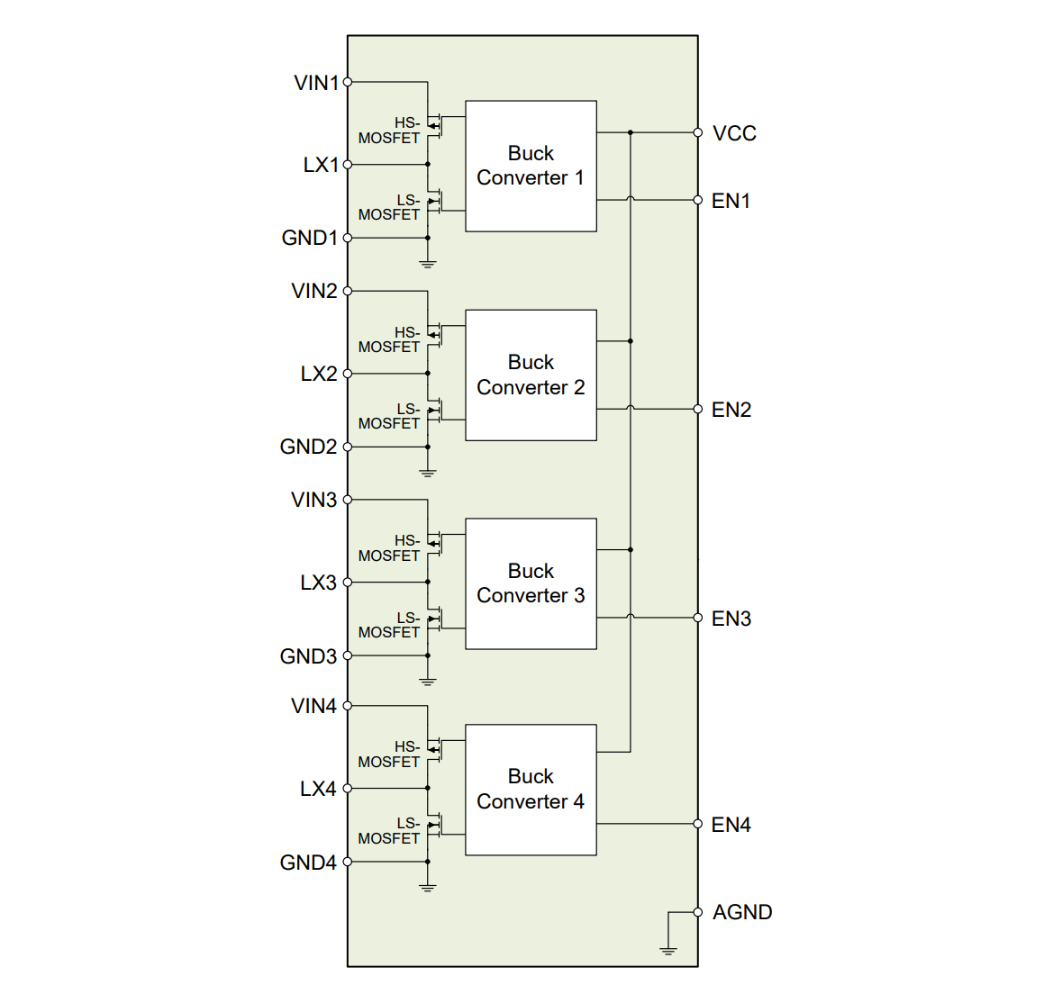
EA3059 is a 4-channel PMIC designed for applications powered by lithium batteries or a 5V DC source. It integrates four synchronous buck converters that deliver high-efficiency output under both light and heavy loads. The internal compensation architecture simplifies application circuit design. Additionally, independent enable control facilitates power sequencing. EA3059 is packaged in a 24-pin QFN 4x4 format.
Project Repository: Collection_of_Power_Module_Design/PMIC/EA3059
Project Online Preview:
Key Features
- Input Voltage and Control Circuit Voltage: 2.7-5.5V
- Output Voltage (4 Buck Converters): 0.6V-Vin
- Output Current: 2A continuous, 4A peak per channel (total output across 4 channels must be less than 10W)
- Fixed 1.5MHz switching frequency
- 100% duty cycle output
- Efficiency of up to 95% per channel
- Standby Current: <1uA
- Independent enable control for each channel
- Internal compensation
- Cycle-by-cycle current limit
- Short-circuit protection
- Self-recovery over-temperature (OTP) protection
- No input over-voltage (OVP) protection (compared to EA3059)
- Packaged in a 24-pin 4mm x 4mm QFN format
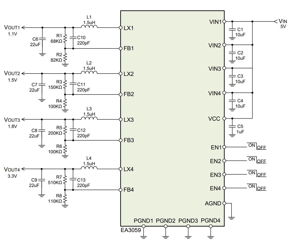
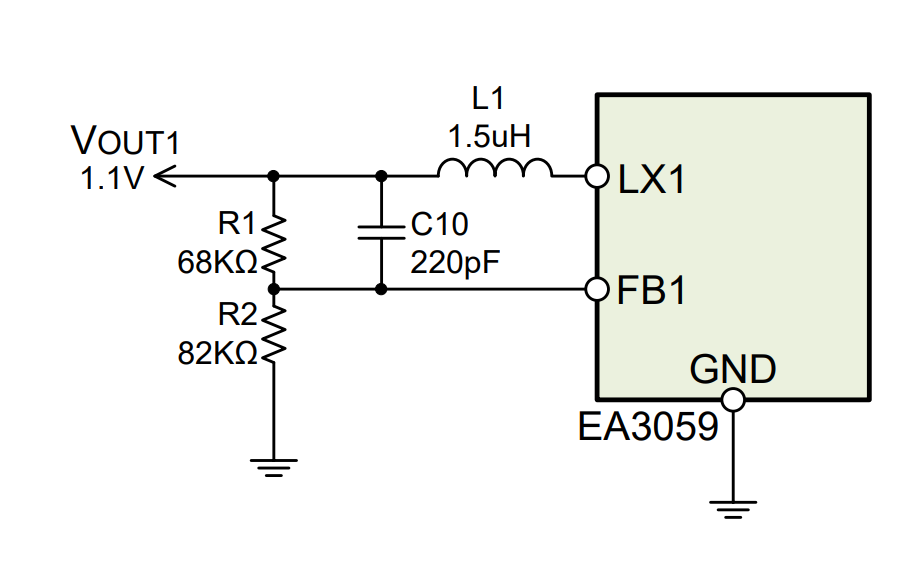
Typical Application Circuit
Internal Functional Block Diagram
Pin Definitions
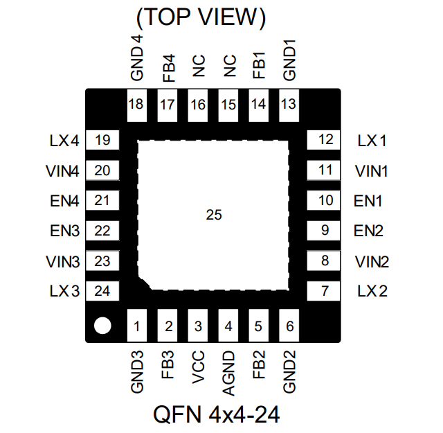
| Pin Name | Pin Description |
|---|---|
| VCC | Power input for internal control circuit |
| VINx | Power input for channel x, decoupled with 10uF MLCC capacitor |
| LXx | Output of the internal MOS switch for channel x, can be connected to a low-pass filter circuit for more stable voltage output |
| FBx | Feedback pin for channel x, connected to voltage output via a voltage divider circuit |
| ENx | Enable pin, must not be left floating |
| GNDx | Ground for channel x |
| AGND | Analog ground |
| Bottom Pads | Ground for heat dissipation, should be connected to ground |
| NC | No connection |
Feature Description
PFM/PWM Mode
Each Buck channel in the EA3059 can operate in PFM/PWM modes. If the output current is less than 150mA (typical value), the regulator will automatically enter PFM mode. In PFM mode, the output voltage and output ripple are higher compared to the PWM mode. However, in light load conditions, PFM is more efficient than PWM.
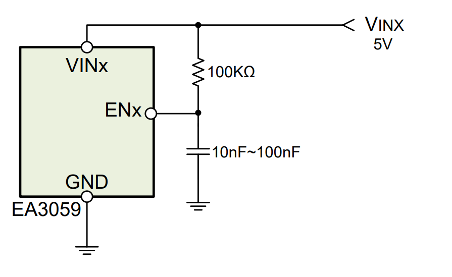
Enable Switch
The EA3059 is a power management IC designed specifically for OTT applications, featuring four 2A synchronous Buck channels that can be individually enabled or disabled using separate EN pins.
If you need to set the turn-on time for each Buck channel, you can program it using the following circuit:
180° Phase-Shift Architecture
To reduce input ripple current, the EA3059 employs a 180° phase-shift architecture. Buck1 and Buck3 share the same phase, while they are 180° out of phase with Buck2 and Buck4. This helps to minimize ripple current and, in turn, reduces EMI.
Overcurrent Protection
Each of the four regulators inside the EA3059 has its own cycle-by-cycle current limiting circuit. When the inductor peak current exceeds the current limit threshold, the output voltage starts to drop until the FB pin voltage is below the threshold, typically 30% lower than the reference value. Once the threshold is triggered, the switching frequency reduces to 350KHz (typical value).
Thermal Shutdown
If the chip temperature exceeds the thermal shutdown threshold, the EA3059 will automatically shut down. To prevent unstable operation, the hysteresis for thermal shutdown is approximately 30°C.
Output Voltage Adjustment
The output voltage for each regulator can be adjusted using a resistor divider network (R1, R2). The output voltage is calculated using the following formula:
If you need to obtain common output voltage values, you can refer to the following table for resistor divider configurations (using 1% precision resistors):
| Output Voltage | R1 | R2 |
|---|---|---|
| 3.3V | 510kΩ | 110kΩ |
| 1.8V | 200kΩ | 100kΩ |
| 1.5V | 150kΩ | 100kΩ |
| 1.1V | 68kΩ | 82kΩ |
Input/Output Capacitor Selection
Input capacitors are used to suppress input voltage noise and provide stable, clean DC input to the device, while output capacitors help suppress output voltage ripple. Both input and output capacitors can be MLCC capacitors (low ESR).
Recommended part numbers for input/output capacitors are as follows:
| Part Number | Capacitance | Voltage | Package |
|---|---|---|---|
| C2012X5R1A106M | 10uF | 10V | 0805 |
| C3216X5R1A106M | 10uF | 10V | 1206 |
| C2012X5R1A226M | 22uF | 10V | 0805 |
| C3216X5R1A226M | 22uF | 10V | 1206 |
Output Inductor Selection
The choice of output inductor primarily depends on the ripple current through the inductor, denoted as ΔI_L. A larger ΔI_L leads to larger output voltage ripple and losses. While smaller inductors can save costs and space, larger inductor values result in smaller ΔI_L, reducing output voltage ripple and losses. The formula for calculating inductance is as follows:
For most applications, EA3059 can use inductors with values between 1.0uH to 2.2uH.
Power Consumption
The total power consumption of EA3059 should not exceed 10W, calculated as follows:
Layout Considerations
The layout for the PMIC requires careful consideration. You can follow the following recommendations to achieve optimal performance:
- It is recommended to use a 4-layer PCB layout, with the LX plane and output plane placed on the top layer, and the VIN plane placed on an inner layer.
- The ground pins of the top layer input/output surface mount capacitors should be connected to the inner layer ground and bottom layer ground through vias.
- AGND should be directly connected to the internal ground plane through vias.
- Try to widen the paths for high current traces.
- Place input capacitors as close as possible to the VINx pins to reduce noise interference.
- Keep the feedback path (from VOUTx to FBx) away from noise nodes (such as LXx). LXx is a high current noise node. Use short and wide traces for the layout.
- Multiple vias should be used to connect the chip's bottom pads to the inner and bottom layer grounds for heat dissipation.
- Place input capacitors as close as possible to the VINx pins to reduce noise interference.
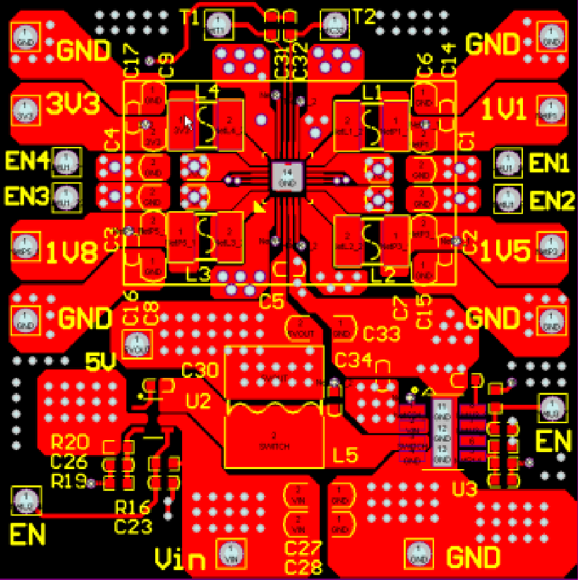
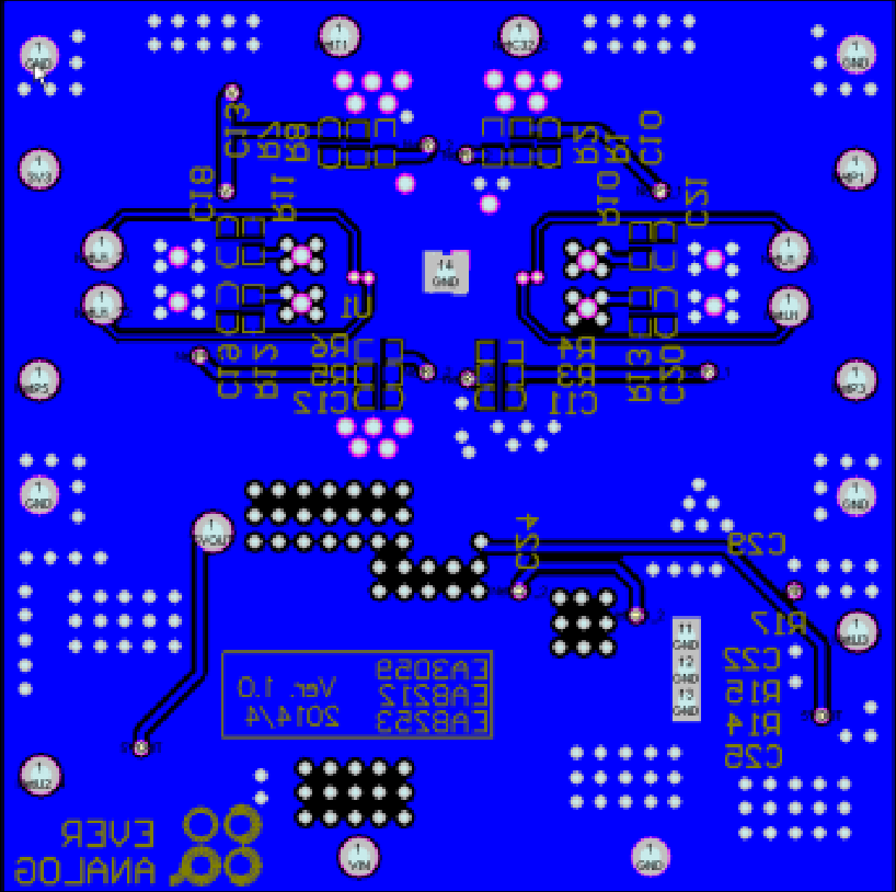
Layout reference is as follows:
Top Layer:
Middle Power Layer:
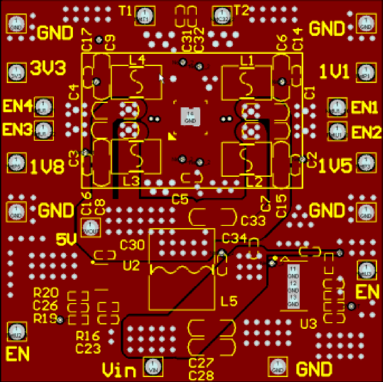
Middle Ground Layer:
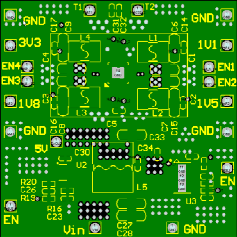
Bottom Layer:
References and Acknowledgments
Original: https://wiki-power.com/ This post is protected by CC BY-NC-SA 4.0 agreement, should be reproduced with attribution.
This post is translated using ChatGPT, please feedback if any omissions.