Differences and Connections Between SWD and JTAG
As we all know, SWD and JTAG are common interfaces for programming and debugging microcontrollers. They share the following features:
- Voltage Range: 1.2 V - 5.5 V
- Clock Speed: Configurable up to 10 MHz
- SWO Trace Capture: Data rate of up to 50 Mbit/s (UART/NRZ mode)
- Isolation Voltage: 1 kV
- Hot Plug Support: Yes
JTAG
JTAG, short for Joint Test Action Group, is defined by the IEEE Standard 1149.1-1990 as of the latest update at the time of this writing.
Here is the topology diagram (daisy chain) for JTAG:
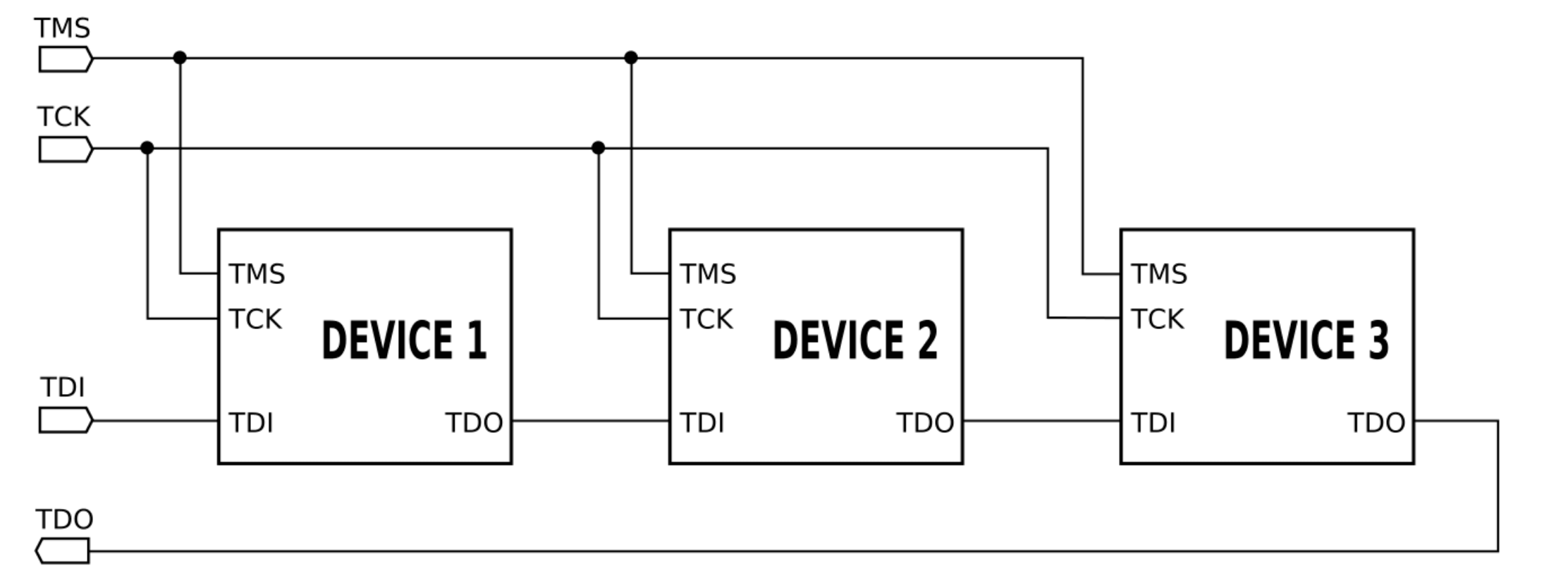
JTAG typically uses 5 pins:
- TDI (Test Data In): Serial input pin
- TDO (Test Data Out): Serial output pin
- TCK (Test Clock): Clock pin, usually with a 100k pull-down resistor
- TMS (Test Mode Select): Mode select (control signal) pin
- TRST (Test Reset): Reset pin
Advantages of JTAG:
- Not limited to ARM series chips
- Has more versatile applications for programming, debugging, and production testing
SWD
Serial Wire Debug (SWD) is a protocol designed specifically by ARM and is primarily supported by ARM devices, making it perform better in ARM microcontrollers.
SWD typically uses 2 pins:
- SWDIO (Serial Wire Data Input Output): Serial data input/output pin
- SWCLK (Serial Wire Clock): Serial wire clock pin
Advantages of SWD:
- Uses fewer pins, only requiring SWDIO and SWCLK
- SWD has special features, such as printing debugging information
- Compared to JTAG, SWD offers better overall performance in terms of speed
Compatibility Between JTAG and SWD
In general, microcontroller boards are equipped with programming connectors that can be compatible with both JTAG and SWD simultaneously. Here is an example:
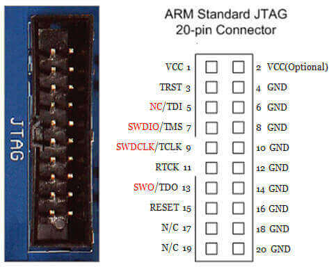
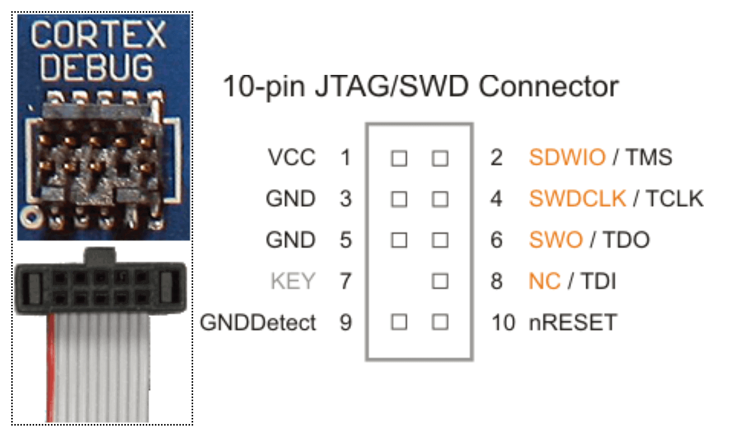
- TCK is compatible with SWCLK
- TMS is compatible with SWDIO
- (TDO is compatible with SWO)
Reasons for choosing SWD over JTAG:
- Circuit schematic design needs to be simple and testable without JTAG functionality.
- PCB has size constraints, and SWD can save space.
- The MCU no longer has extra pins available for JTAG.
References and Acknowledgments
- Differences Between SWD and JTAG Debugging Interfaces
- Cortex JTAG, SWD Debug Port Sharing
- JTAG/SWD Interface
- JTAG
Original: https://wiki-power.com/ This post is protected by CC BY-NC-SA 4.0 agreement, should be reproduced with attribution.
This post is translated using ChatGPT, please feedback if any omissions.